Electronics Build Up
Jul 15, 2013 @ 9:11pm
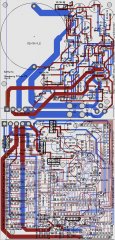
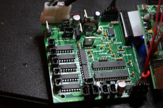
Making an electronics package this complicated pretty much required that I have a proper PCB produced instead of trying to use a protoboard or something. Turns out getting a board made is not expensive, it was about $75 from ITEADstudio. Using the gEDA tools I could make all the schematics and then convert those schematics to the right formats needed for the prototype PCB.
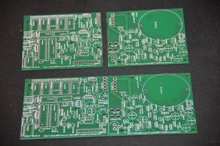
For the schematics I used gschem, I had to create many of the symbols, the files I used are at the bottom of the page. The layout was then performed by generating a .pcb file from the top level using gsch2pcb, and I did the layout with that. The end result is both the power supply and interface board on one 5x10cm 2-layer board.
After sending the files to the shop and a few weeks of waiting I got the finished board. I used a dremel to separate them and had could start soldering everything together.
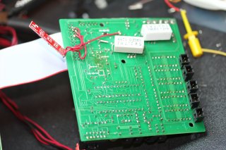
Unfortunately soldering everything didn't go as planned. The number one thing I learned is I need to quadruple check clearances on everything! Connectors need a lot of clearance, guessing didn't cut it at all. I wasn't even close, I had to put connectors on the bottom of the board to make them fit.
Along the same lines of clearances, many other things just didn't fit, half the things I made my own footprint for were too tight. Specifically the switching power supply chip and power diodes didn't fit, I ended up sniping the leads and soldering them like SMT devices. The AC adapter connector was also the wrong size (and I thought I did check the size for that). Also, heatsinks ended up being mostly an afterthought, but turns out they really do need a LOT of space, the heatsinks really should be one of the first things done when laying out the PCB. In the end, PCB footprints are something that really needs to be right.
Testing
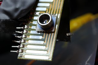
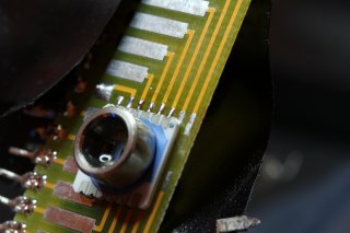
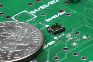
After buildup, it was time to test it, as I stated in my earlier post the 5V PS had problems that I had to fix. Another problem was the pressure sensor. Originally I used a MS5541-CM, but my plan to solder wires to it directly failed miserably, the second wire ripped the pad right off it. The replacement was a MS5535-CM, which while somewhat more expensive, is more accurate and bigger (making it easier to work with and find a tube that I can connect to it), it also wasn't out of stock. Soldering it to a SMT adaptor board worked just fine. At least it appears to, I haven't finished the code to interface with it just yet.
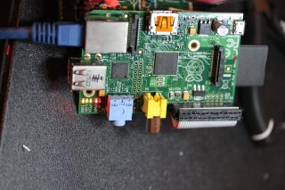
The last major problem I found was I miswired the GPIO header, and connected that to the accelerometer interrupt output pin to the 3.3V raspberry pi supply. Obviously not good, so I simply snipped that pin off the interface board header to disconnect it. In the end it turned out not to matter as I couldn't solder the accelerometer on anyways. Testing is obviously going to continue as code development continues, but for now I have verified that all I2C devices show up, and I have working code that communicated with the AVR.
root@raspberrypi:~/sub# i2cdetect -y 1
0 1 2 3 4 5 6 7 8 9 a b c d e f
00: -- -- -- -- -- -- -- -- -- -- -- -- --
10: -- -- -- -- -- -- -- -- -- -- -- -- -- -- 1e --
20: 20 21 -- -- -- -- -- -- -- -- -- -- -- -- -- --
30: -- -- -- -- -- -- -- -- -- -- -- -- -- -- -- --
40: -- -- -- -- -- -- -- -- -- -- -- -- -- -- -- --
50: -- UU -- 53 -- -- -- -- -- -- -- -- -- -- -- --
60: -- -- -- -- -- -- -- -- 68 -- -- -- -- -- -- --
70: -- -- -- -- -- -- -- --
Downloads
The schematics here are the schematics used to generate the PCB files, they have errors as documented elsewhere in previous posts. The -pcb tarball contains the actual .pcb file generated by the pcb program. The gerber files are the files that were sent off for production. But if anyone is interested they are good starting points. I will release updated versions of at least the schematics by the time I finish the project (and know all problems).
subIO-schematics-revA.tar.bz2
subIO_revA-pcb.tar.bz2
subIO_revA-gerber.tar.bz2
